Full-Stack Technology Loop
From MicroLED emission, microlens coupling, and fiber transmission to PD reception — mastering the complete technology chain for end-to-end optimization.

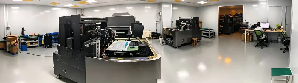
From MicroLED emission, microlens coupling, and fiber transmission to PD reception — mastering the complete technology chain for end-to-end optimization.
Built on 16nm–130nm mature CMOS processes, directly leveraging the semiconductor industry infrastructure — no specialized fab investment required.
Array-parallel architecture scales linearly — every additional channel adds incremental bandwidth, breaking the per-channel rate ceiling.
Our team spans photonics, semiconductor devices, system architecture, and AI hardware. Core members bring full-stack R&D experience from materials science to system integration, focused on translating cutting-edge photonics research into mass-manufacturable data center interconnect products.
Please send your resume to our recruitment email (check the website for updates)